
SEM imaging and EDS elemental analysis
High-magnification images of surfaces, fractures, particles, and coatings, plus which elements are present and where. Scoped by a PhD scientist, run at UC San Diego's Nano3 facility, and quoted at a fixed price before you ship. No minimum job size.
What SEM shows you
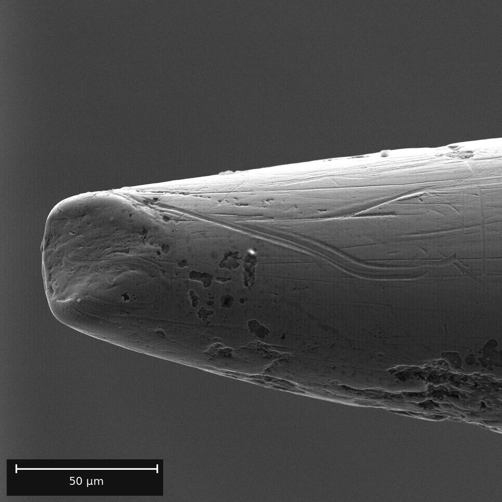
A scanning electron microscope images a surface at magnifications far beyond a light microscope, with much greater depth of field. It's the fastest way to see what a fracture, coating, powder, or defect actually looks like.
Typical questions
- Why did this part crack, and where did the fracture start?
- Are there voids, delamination, or contamination on this surface?
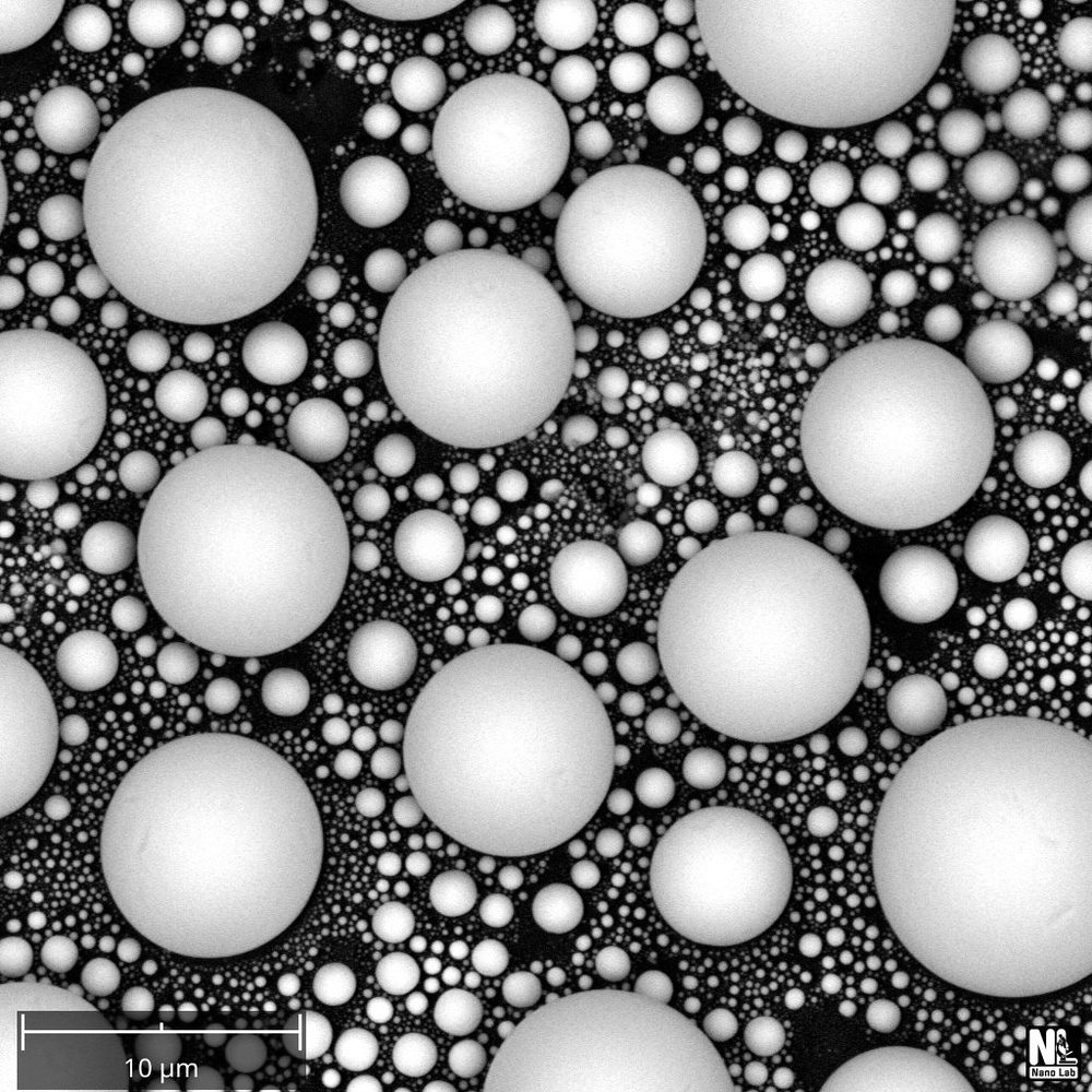
- What are the size and shape of the particles in this powder?
- Does this batch look like the last good one?
Good to know
- Insulating samples are usually coated with a thin conductive layer. Low-vacuum imaging is available when coating isn't an option.
- SEM shows the surface. To see below it, ask about FIB-SEM or polished cross-sections.
- Reading fracture surfaces is a specialty: see our note on SEM fractography.
What EDS adds
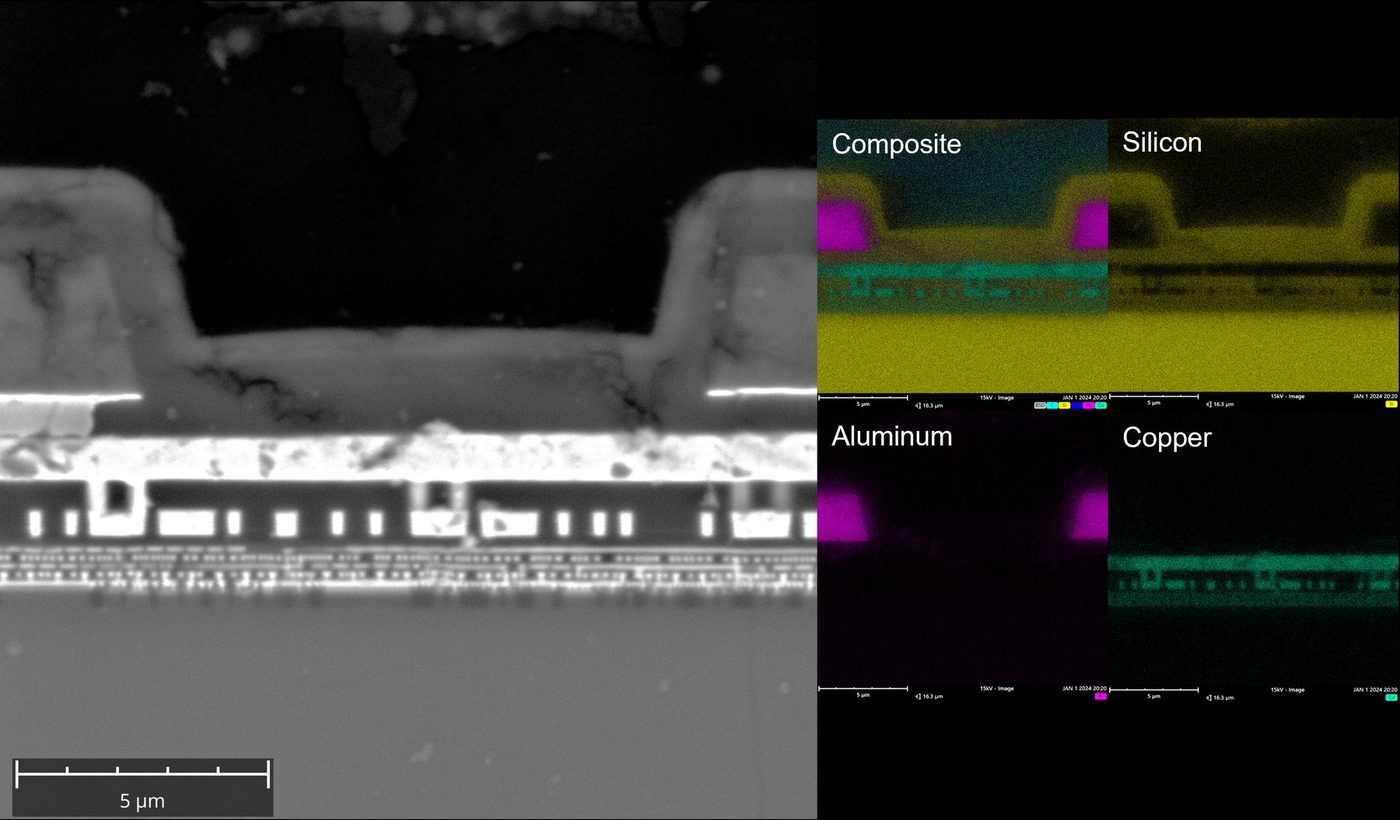
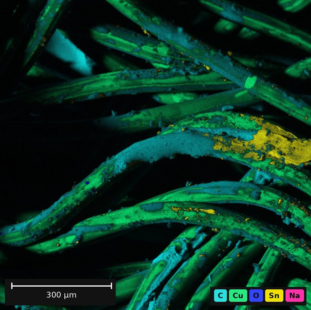
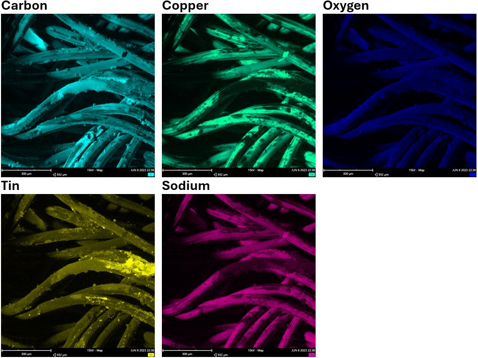
Energy-dispersive X-ray spectroscopy runs in the same instrument. The electron beam makes each element give off X-rays at its own energies, so EDS tells you which elements are present, roughly how much of each, and where they sit: at a single spot, along a line, or as a map across the image.
Typical questions
- What is this particle, residue, or discoloration made of?
- Is the plating or coating where it should be, and is it uniform?
- Which elements are at this interface or in this inclusion?
Good to know
- EDS is semi-quantitative. It does not certify an alloy grade.
- Light elements are difficult, and carbon is unreliable because of surface contamination.
- The signal comes from up to a few micrometers below the surface, so thin films are averaged with what's under them. For the top few nanometers, see XPS.
- EDS gives elements, not compounds. For polymers and organics, see our note on identifying unknown materials.
How it works
- Tell us the question. A photo and a sentence about what you need to know is enough to start. We reply within one business day.
- Fixed quote. We say what will be imaged and analyzed, and what you'll receive, before you ship. One sample is a real job.
- Analysis. Our team runs the SEM at UC San Diego's Nano3 facility, typically within three to five business days of your samples arriving.
- Results. You get the image and data files and a PDF report of what was observed and measured, with the methods used. See an example report.
SEM & EDS questions
Can you image samples that don't conduct electricity?
Yes. Insulating samples such as polymers, ceramics, and glass are usually given a thin conductive coating first. If a sample can't be coated, low-vacuum imaging is available. Tell us which you'd prefer.
How small a feature can you see?
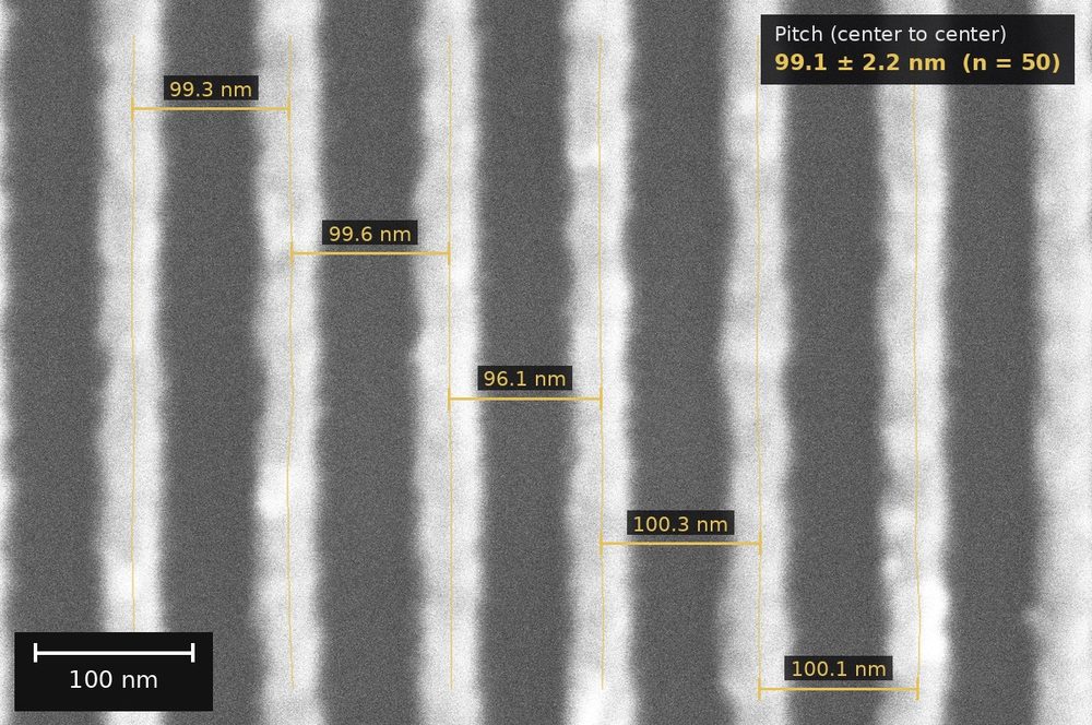
It depends on the sample, but well below a micrometer is routine. Our example images include a calibration standard with a 100 nm line pitch, resolved and measured line by line.
Can EDS tell me the alloy grade?
No. EDS is semi-quantitative: it reliably shows which elements are present and roughly how much, but not the precise composition needed to certify a grade.
Spot analysis, line scan, or map?
All three. Spot analysis identifies a particle or inclusion, line scans show how composition changes across an interface, and maps show where each element sits across an area.
How big can the sample be?
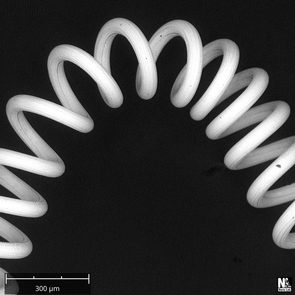
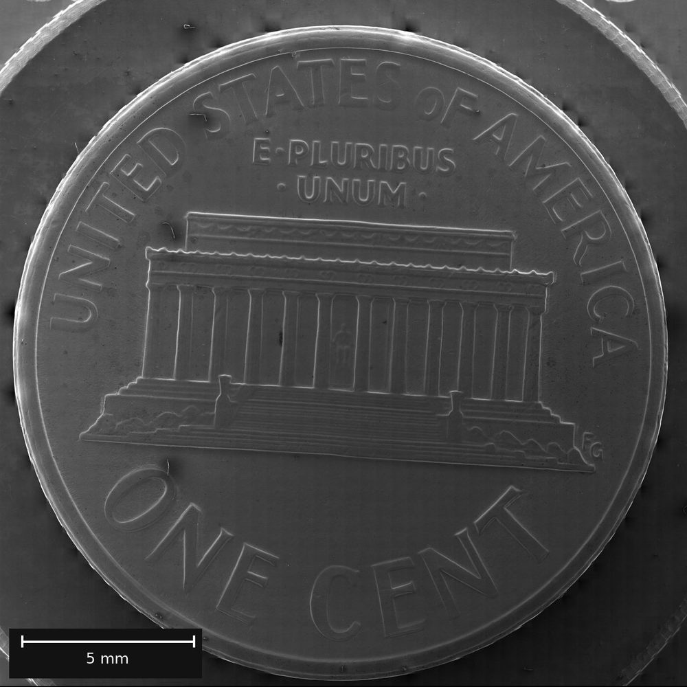
Small parts usually go in whole; our examples include an entire one-cent coin. Larger parts may need to be cut down, which we agree with you before cutting.
How fast?
We reply within one business day and usually quote SEM/EDS the same or next business day. Three to five business days after samples arrive is typical.
Have a sample and a question?
Email a short description, and a photo if you have one. We reply within one business day. Most SEM, FIB, XPS and XRD quotes go out the same or next business day; other techniques take a few business days while we confirm the method and scheduling.
Or email info@nanolab.llc