Services
Most of our work, especially electron microscopy, runs at UC San Diego's Nano3 facility, and our team usually runs the instruments. For some techniques we work with trusted specialists at partner laboratories. Your quote says what will be done, and the price is fixed and the timeline agreed before you ship.
SEM imaging
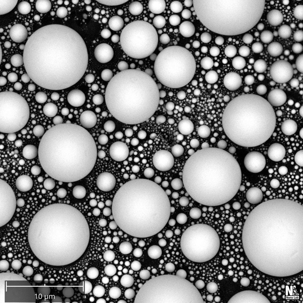
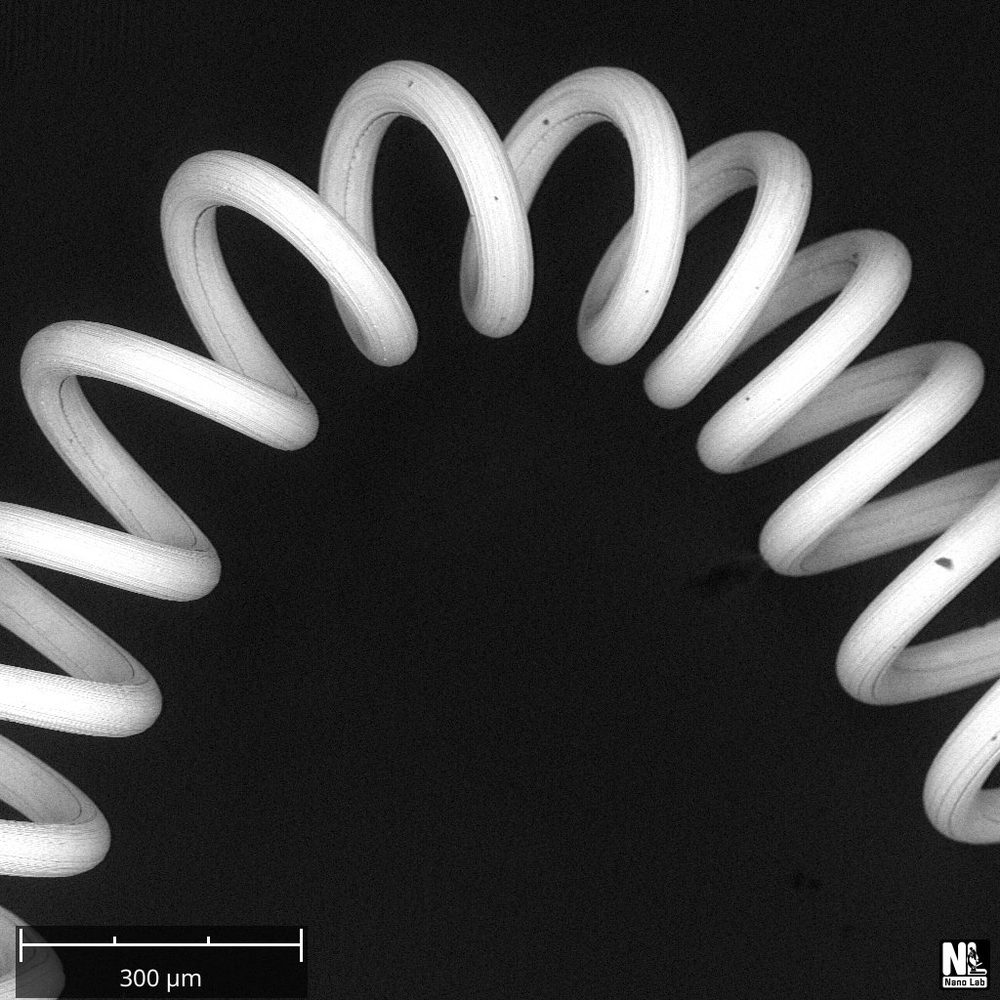
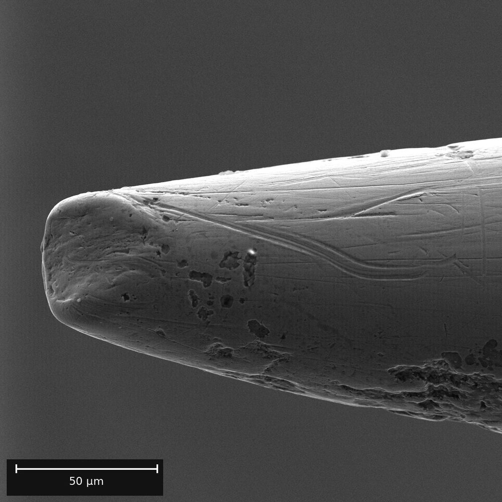
Scanning electron microscopy for surface morphology, fracture surfaces, particles, fibers, coatings, and defects.
Typical questions
- What does the surface or fracture look like at high magnification?
- Are there cracks, voids, delamination, or contamination?
- What are the particle sizes and shapes in this powder?
- How does this batch compare with the last one?
Good to know
- Insulating samples are usually given a thin conductive coating. Low-vacuum imaging is available when a sample can't be coated.
- SEM shows the surface. To see below it, ask about mechanical or FIB-SEM cross-sections.
EDS elemental analysis
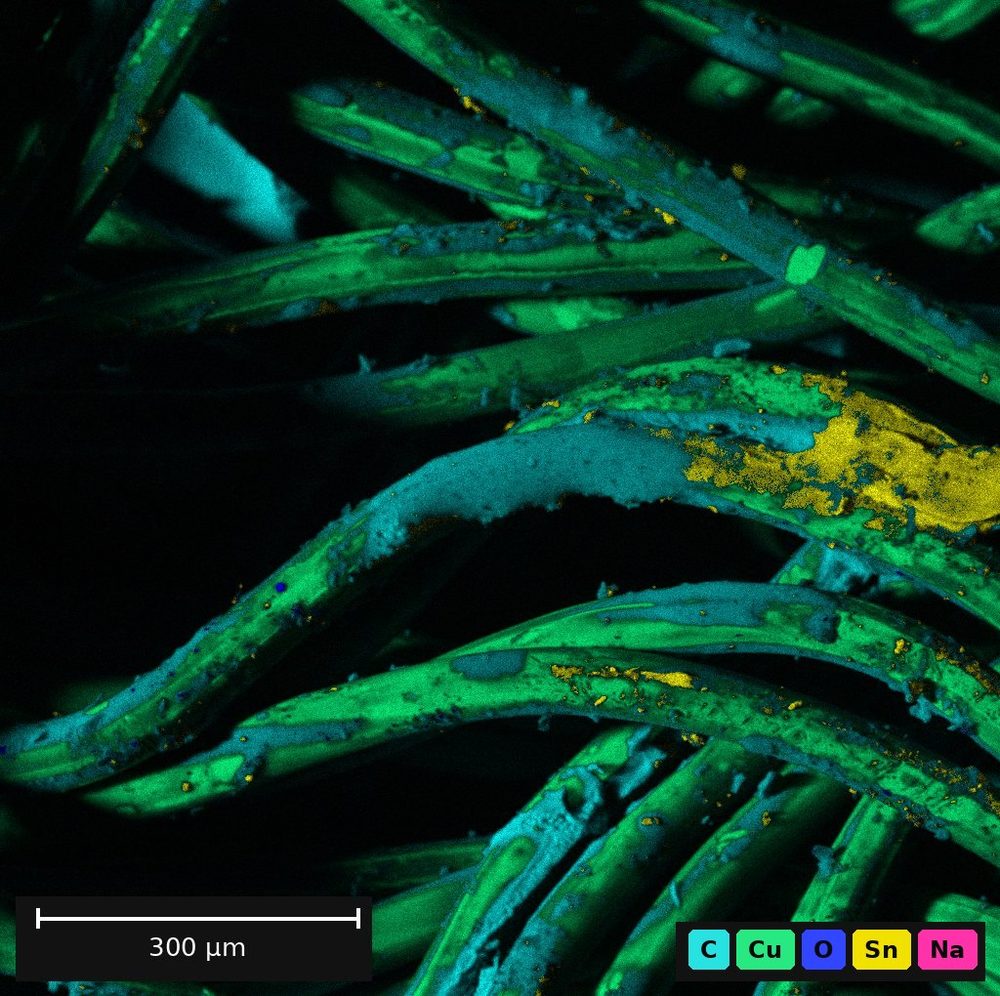
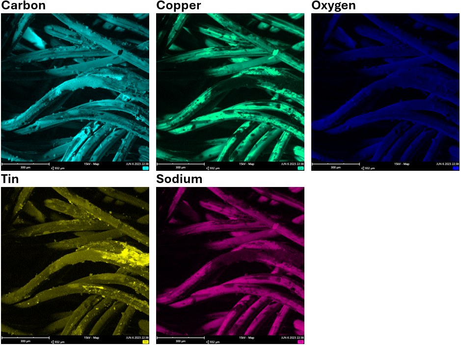
Energy-dispersive X-ray spectroscopy in the SEM: which elements are present, and where.
Typical questions
- What is this particle or residue made of?
- Is the coating composition uniform across the part?
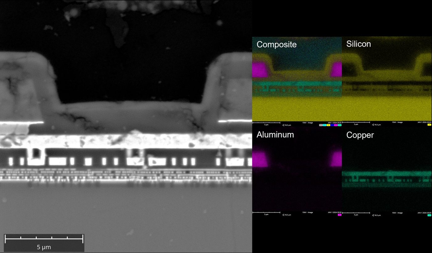
- Where are the elements distributed in a cross-section?
Good to know
- EDS is semi-quantitative. It does not certify an alloy grade.
- Light elements are difficult, and carbon in particular is unreliable because of surface contamination.
- The signal comes from up to a few micrometers below the surface, depending on beam voltage and material, so thin layers are averaged with what is under them.
FIB-SEM cross-sections
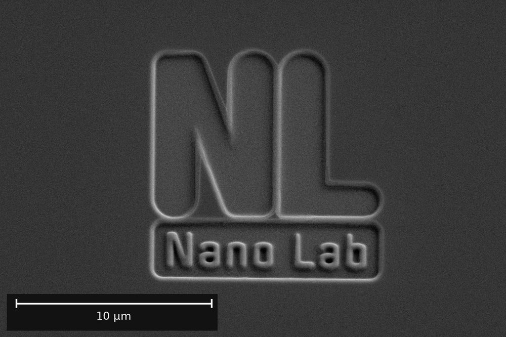
A focused ion beam cuts a precise cross-section at the spot you care about, which is then imaged in the same instrument. EDS on the cross-section is available on request.
Typical questions
- How thick are the coating and each layer, and are they continuous?
- Is there a void, crack, or delamination under this surface feature?
- What does the inside of this particle or bead look like?
Good to know
- Each cross-section is tens of micrometers wide. Tell us if you need to see a larger area.
- Cryo-FIB is available for beam-sensitive materials.
Ground and polished cross-sections
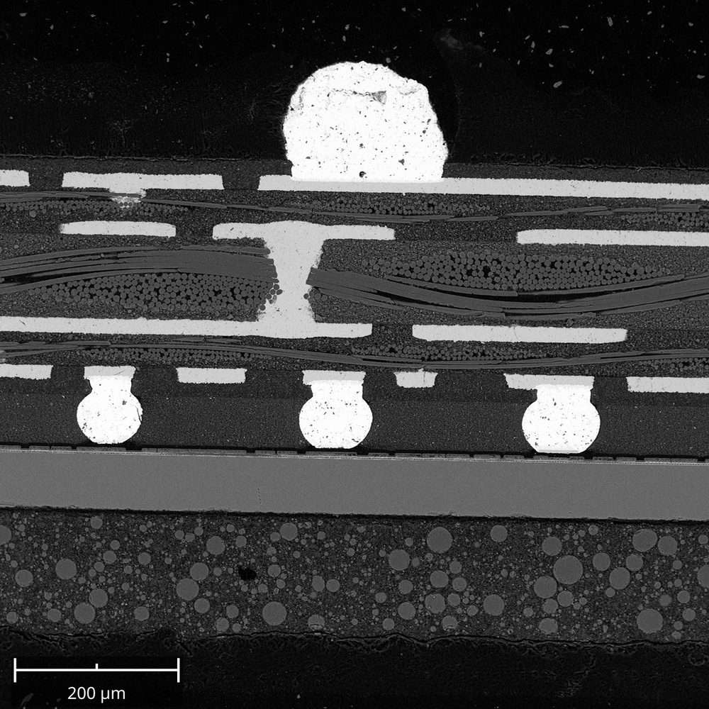
Mechanical cross-sections for when you need to see a larger area than a FIB cut allows: electronic packages, solder joints, coatings, and layered parts, imaged by SEM with EDS on request.
Typical questions
- What does the whole joint, package, or layer stack look like in section?
- Are there voids, cracks, or delamination across the part?
- How do layer thicknesses vary across a larger area?
Good to know
- EDS maps across the section are available on request.
XPS and Auger electron spectroscopy
X-ray photoelectron spectroscopy measures the elements and their chemical states in the top few nanometers of a surface. Auger electron spectroscopy (AES) analyzes much smaller spots.
Typical questions
- What is on this surface: residue, oxide, or contamination?
- Did the cleaning, plasma, or coating step change the surface chemistry?
- What is the chemical state of an element, for example metal or oxide?
Good to know
- Both techniques see only the outermost few nanometers.
- Samples must tolerate high vacuum.
- Hydrogen and helium are not detected.
X-ray diffraction
XRD identifies crystalline phases, estimates how much of each is present, and compares phase makeup between samples.
Typical questions
- Which crystalline phases are present?
- How much of each phase is there?
- Is this batch phase-pure, or are there secondary phases?
- Do two batches have the same phase makeup?
Good to know
- Phase fractions are estimated in weight percent from reference intensity ratios. Ask if you need full Rietveld refinement.
- Amorphous material shows as a broad background, not as identifiable phases.
- Very minor phases can fall below the detection limit.
TEM imaging
Transmission electron microscopy for nanoparticles, thin films, and fine microstructure, at much higher resolution than SEM.
Typical questions
- What are the size and shape of these nanoparticles?
- Is this material crystalline, and is it uniform?
- What does the structure look like at the nanometer scale?
Good to know
- Samples must be electron-transparent. Powders and particles are usually dispersed on a grid.
- FIB lamellae for cross-sectional TEM are prepared through a partner laboratory.
Surface metrology
Laser confocal and stylus profilometry and spectroscopic ellipsometry for thickness, step height, and roughness.
Typical questions
- How thick is this film or coating?
- What is the surface roughness?
- What is the height of this step or feature?
Good to know
- Ellipsometry suits thin, smooth films on reflective substrates.
- Stylus profilometry touches the surface. Optical methods don't.
Chemical, thermal, and particle analysis
Scoped, quoted, and reported the same way as everything else.
- FTIR spectroscopy
- Raman spectroscopy
- Thermal analysis (TGA and DSC)
- X-ray fluorescence (XRF)
- Particle sizing and zeta potential (DLS, NTA)
- BET surface area
- Contact angle
Not listed? Ask. If we can't do it, we'll tell you quickly.
Frequently asked questions
How quickly will I hear back?
Within one business day, with a quote or with questions if we need more detail.
How long does the analysis take?
Three to five business days is typical for core techniques once samples arrive. Larger batches are scheduled with you, and results can be delivered in stages.
How is the work priced?
Every job gets a fixed quote, agreed before you ship. The quote lists what will be done and what you receive.
Is there a minimum job size?
No. One sample is a real job.
Where do I send samples?
The shipping address comes with your quote. If a sample could be hazardous or biological, tell us before shipping so we can confirm whether and how we can take it.
Where is the work done?
Most of our work, especially electron microscopy, runs at UC San Diego's Nano3 facility, and our team usually runs the instruments. For some techniques we work with trusted specialists at partner laboratories.
What do I receive?
The data files and a PDF report of what was observed and measured, with the methods used. Interpretation of the results is available as a separately quoted add-on.
Are you ISO 17025 accredited?
Nano Lab is not ISO 17025 accredited and does not perform testing under GLP or GMP. Our work is built for R&D, failure analysis, and engineering questions, where speed, flexibility, and direct access to the scientist matter most. When a project needs more formality, we can agree on a documented test procedure with you before work begins.
Is my information kept confidential?
Yes. We keep client samples, data, and identities confidential, and we never publish them without written permission.
Reports
Every job comes with the data and a PDF report of what was observed and measured, with the methods used. The report describes; it doesn't speculate. If you want our interpretation of what the results mean, we quote that as a separate add-on. See an example report (PDF) →
Have a sample and a question?
Email a short description, and a photo if you have one. We reply within one business day with a quote, or with questions if we need more detail.
Or email info@nanolab.llc