Examples

Example images

These images are of calibration standards and demonstration samples. We never publish client samples or data without written permission. Click any image to see it full size.

Example report

A full report in our standard format, using the calibration measurement below as the data. Open the example report (PDF) →

FIB
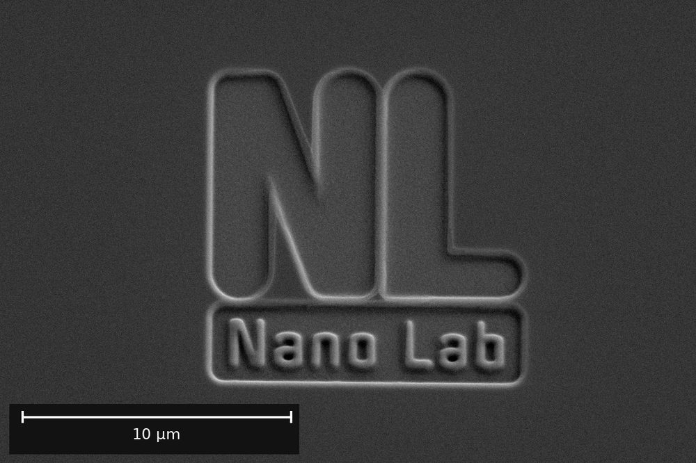
The Nano Lab logo milled into a silicon wafer with a focused ion beam, SEM.

Integrated circuit, polished cross-section, SEM and EDS
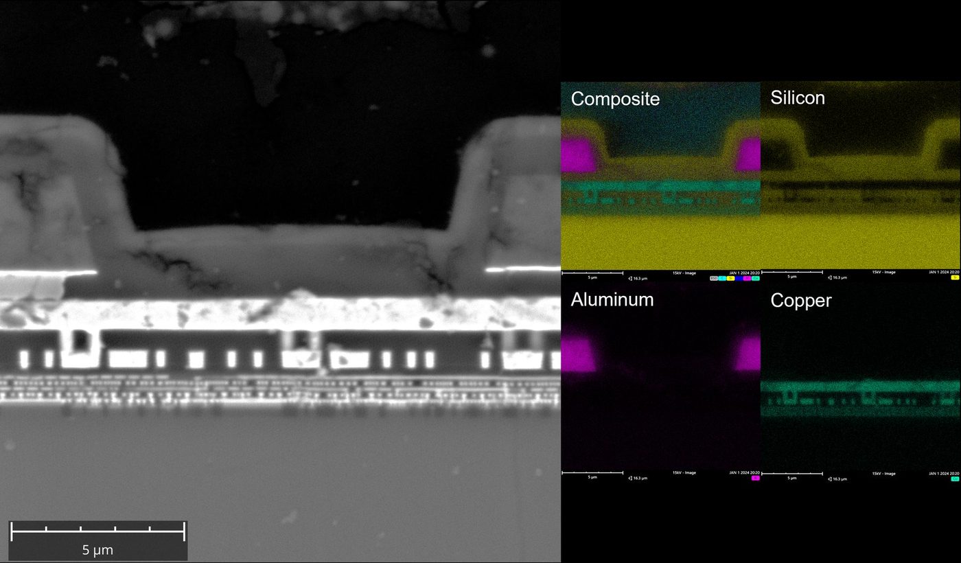
SEM image and EDS elemental maps of a polished integrated circuit cross-section: silicon, aluminum, and copper.

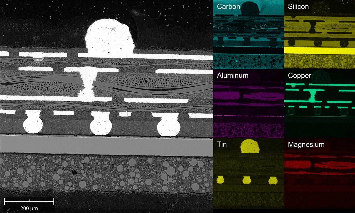
Integrated circuit package, SEM and EDS
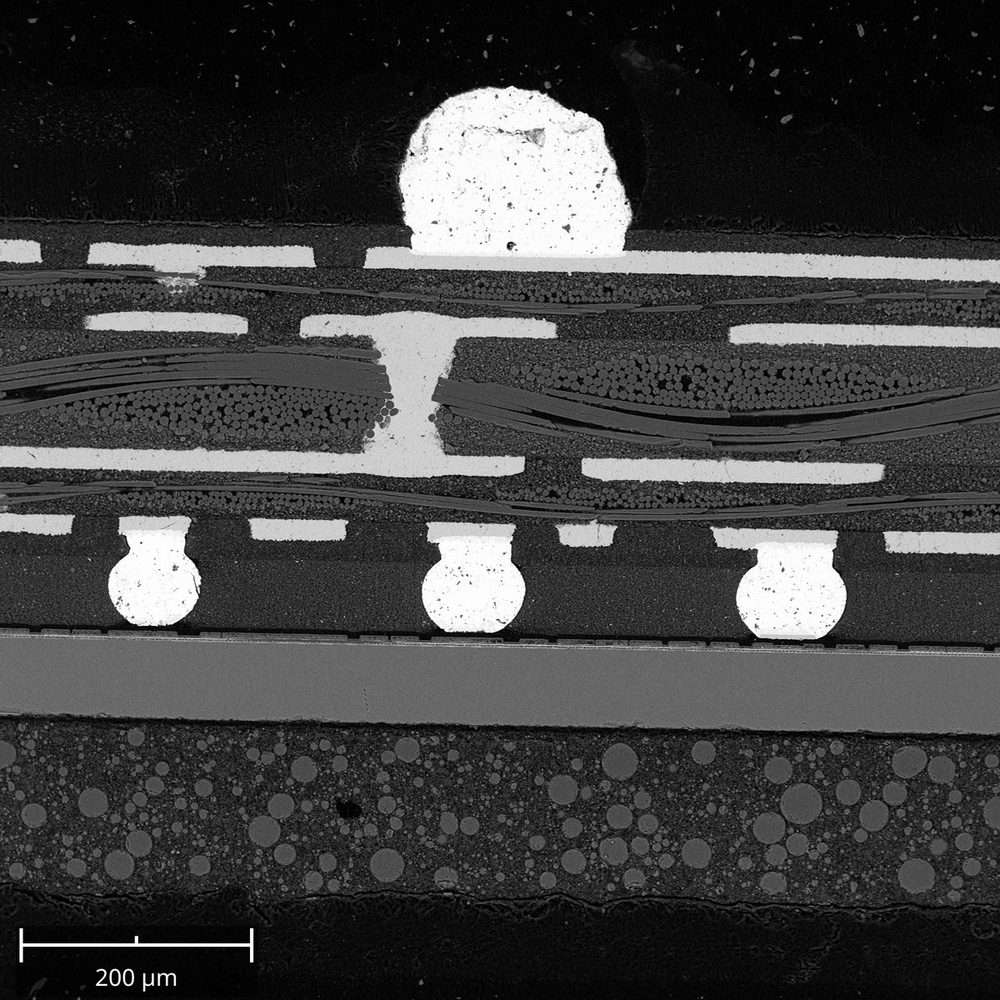
SEM image of a cross-section through an integrated circuit package: solder bumps, copper traces and a via, glass-fiber laminate, and particle-filled mold compound.
SEM image and EDS elemental maps of an integrated circuit package cross-section: carbon, silicon, aluminum, copper, tin, and magnesium.

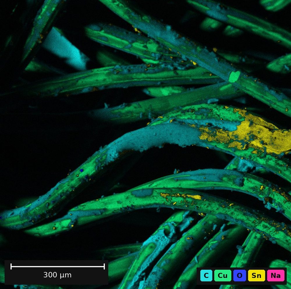
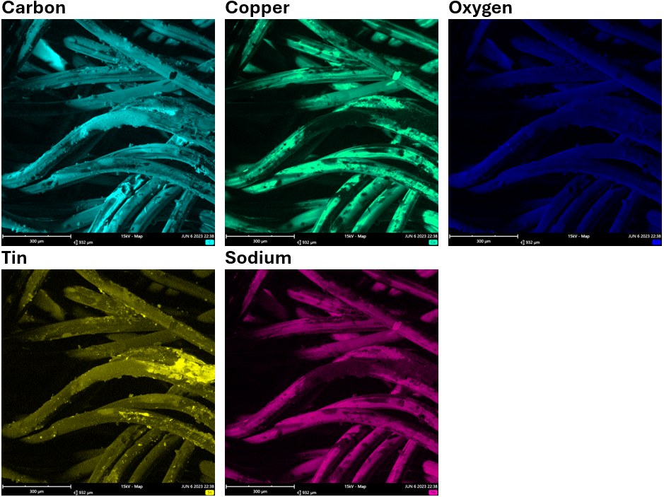
EDS elemental mapping

EDS false-color map of solder on copper solder wick: carbon, copper, oxygen, tin, and sodium.
The same solder wick area, one EDS map per element.

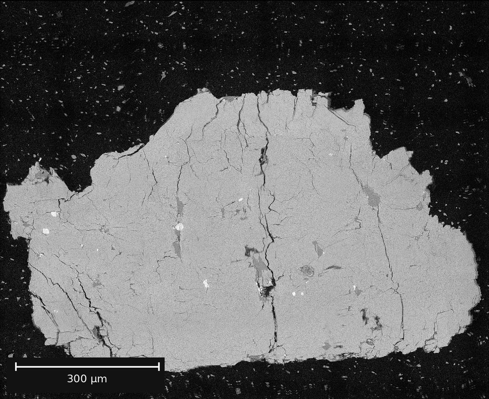
Minerals and particles, SEM

Cross-section of the meteorite NWA 6963, SEM.
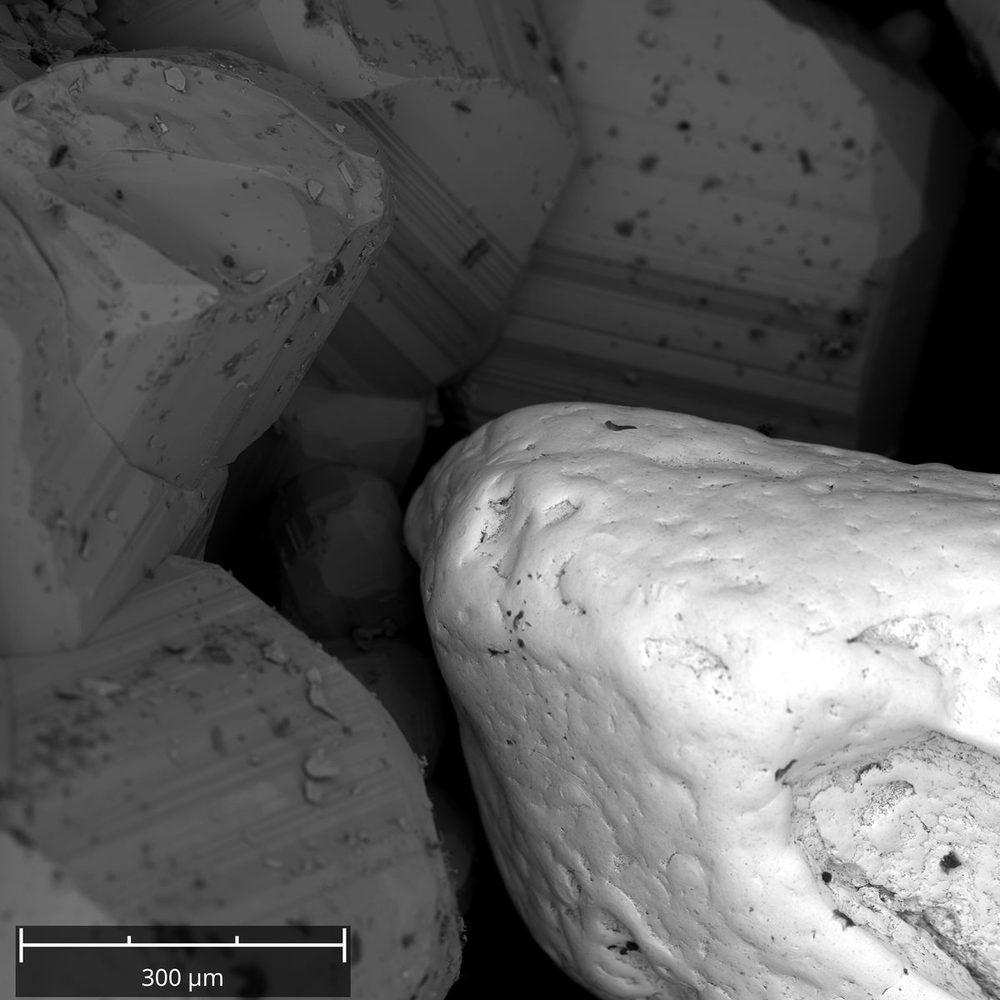
Gold grain (right) next to pyrite crystals, SEM.
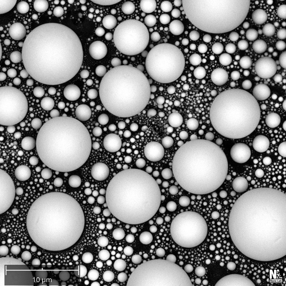
Tin microspheres on carbon, SEM.
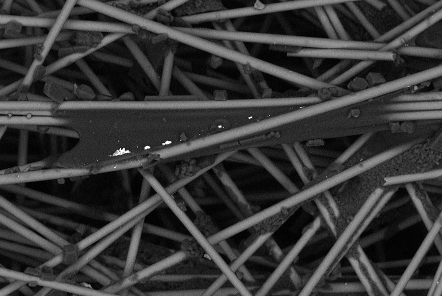
Gold nanoparticles on the test strip of an at-home COVID-19 test (lateral flow assay).
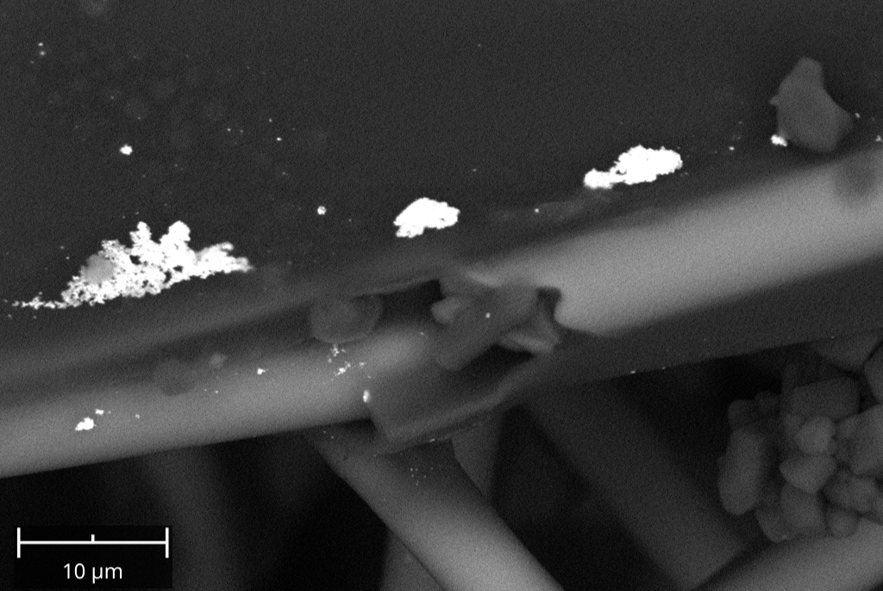
The same lateral flow test strip at higher magnification.

Medical device, false-colored SEM
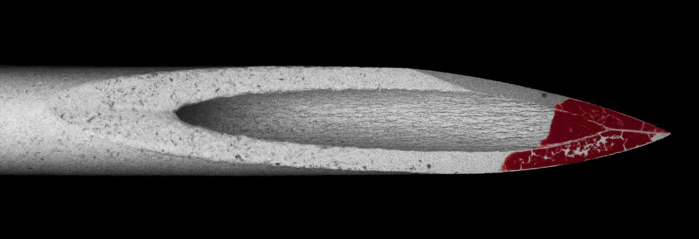
False-colored SEM image of blood on the tip of a hypodermic needle.

Surfaces, fibers, and wires, SEM
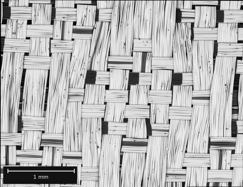
Metallic shielding textile, SEM.
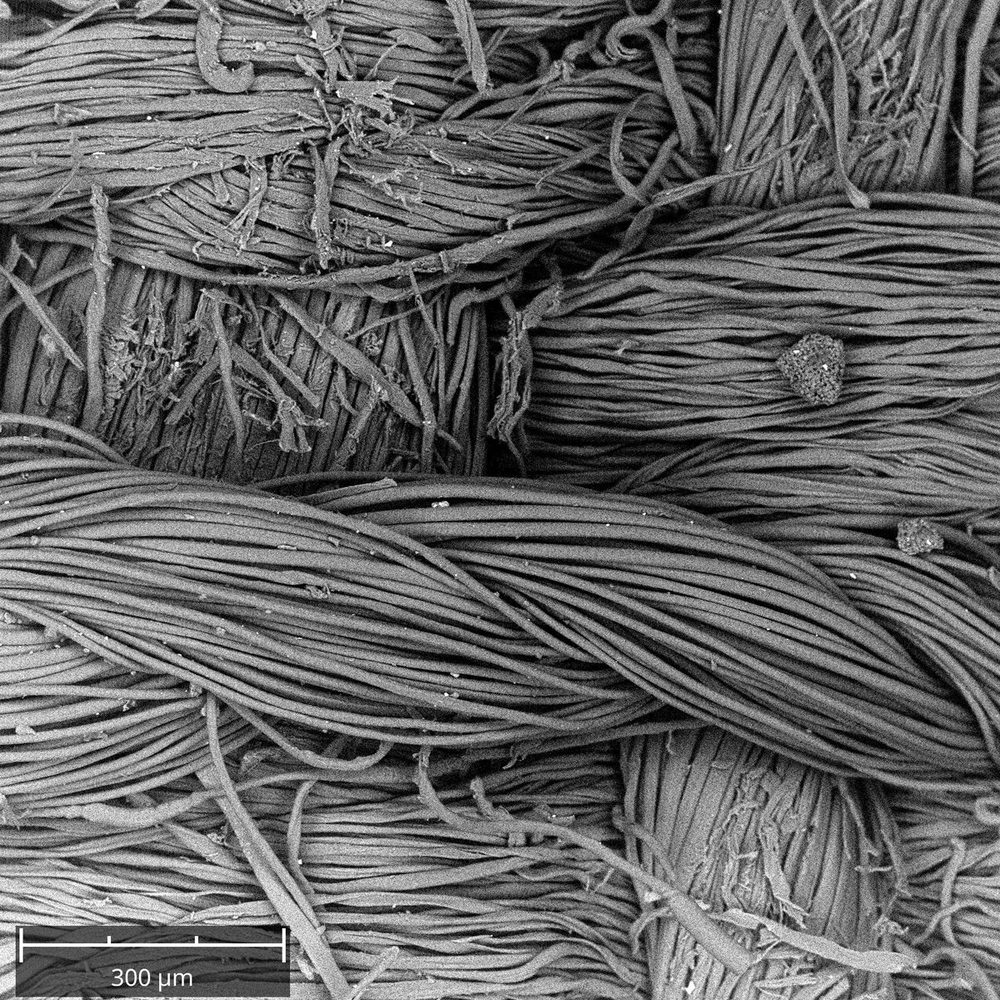
Woven fabric fibers, SEM.
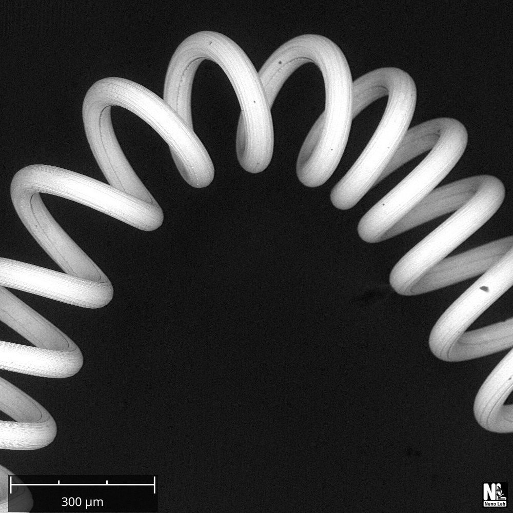
Light bulb filament, SEM.
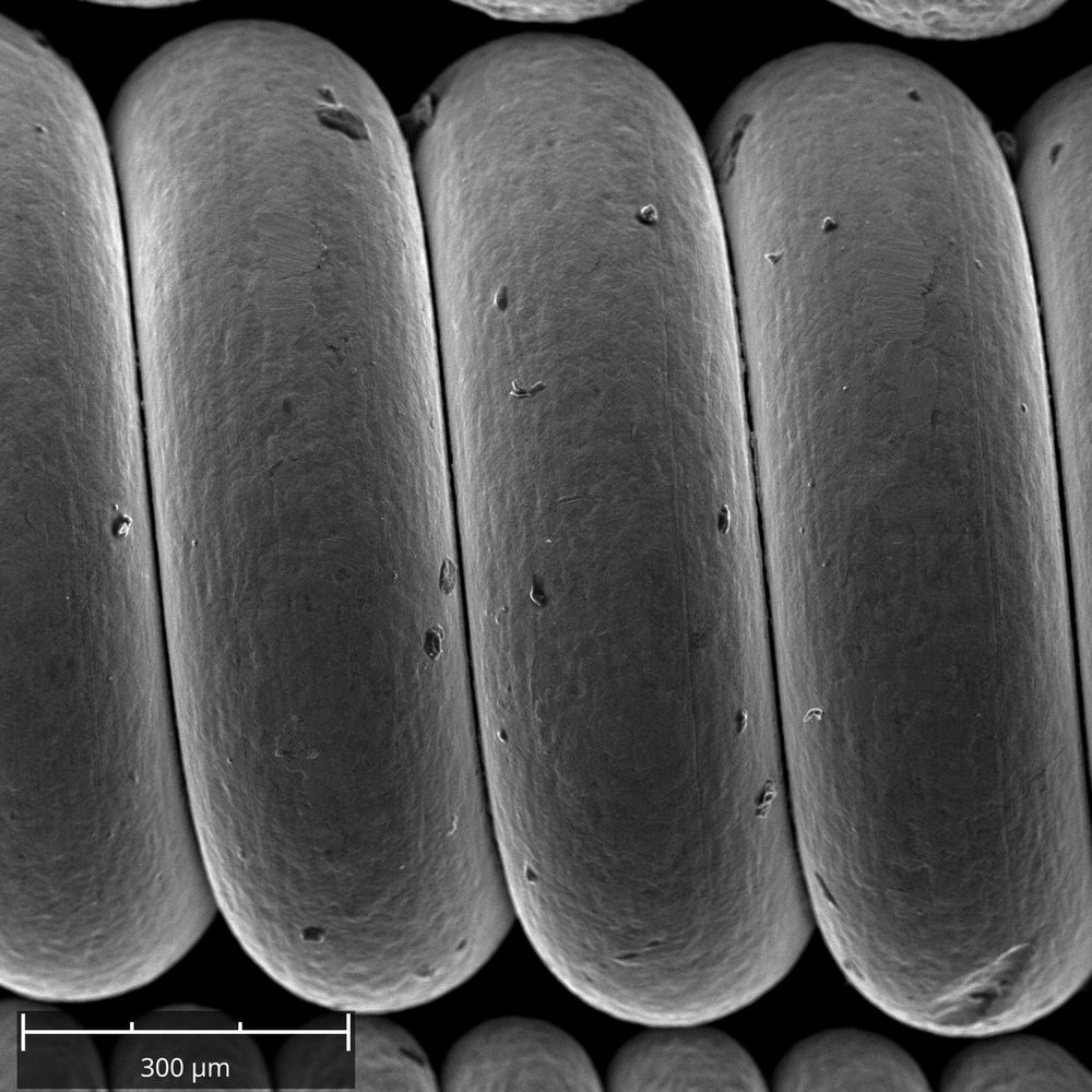
Windings of a guitar string, SEM.
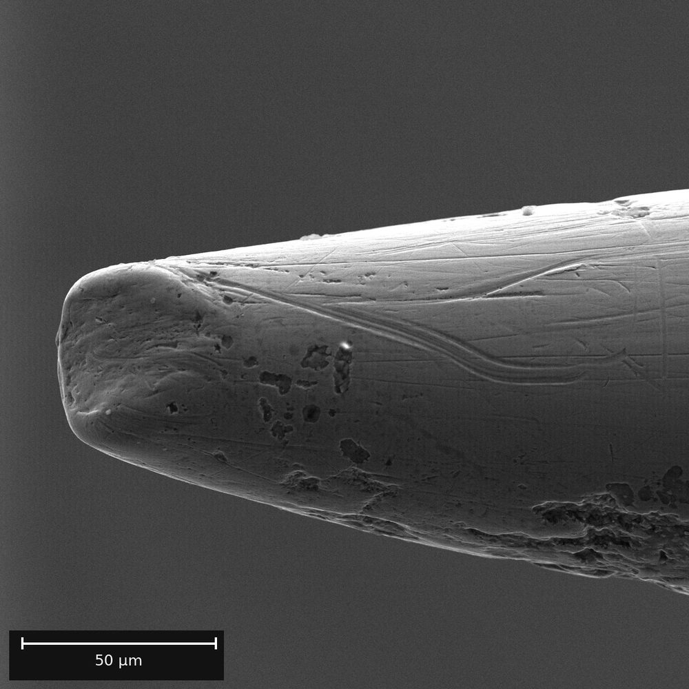
Tip of a needle, SEM.
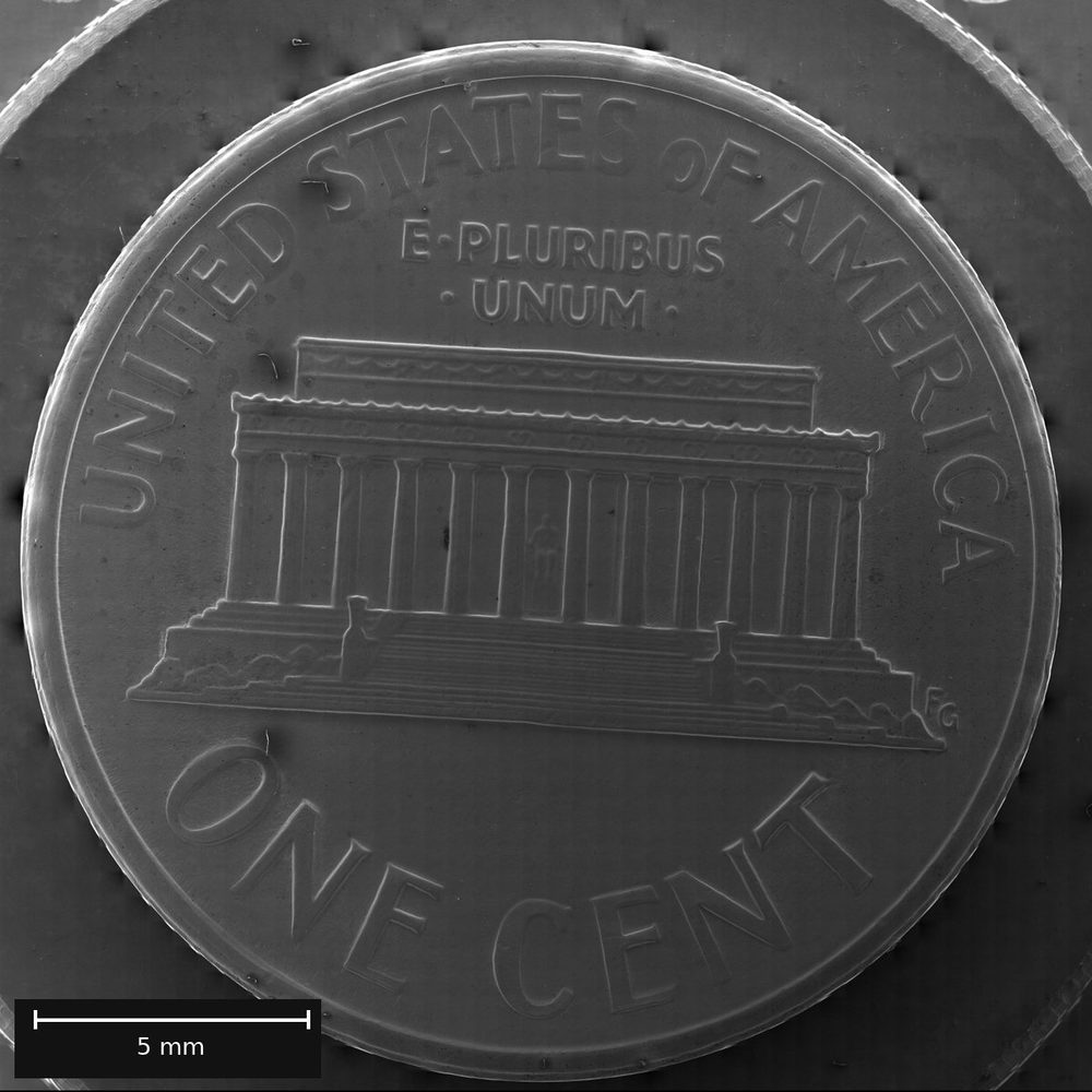
A US one-cent coin imaged whole in the SEM.

SEM calibration standard

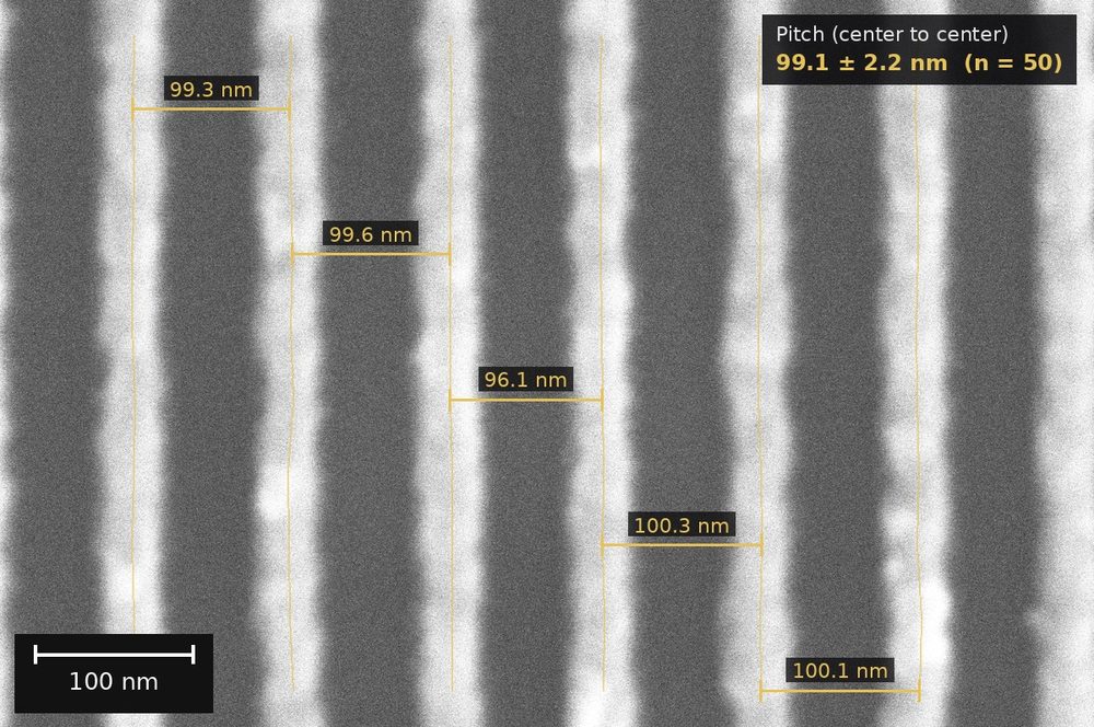
Calibration standard with a nominal 100 nm line pitch, measured center to center as the standard's reference specifies. Mean pitch 99.1 ± 2.2 nm (mean ± SD, n = 50: five adjacent line pairs, each measured at ten positions along the lines). Line centers are the midpoints of each line's full width at half maximum; pixel size 0.45 nm.
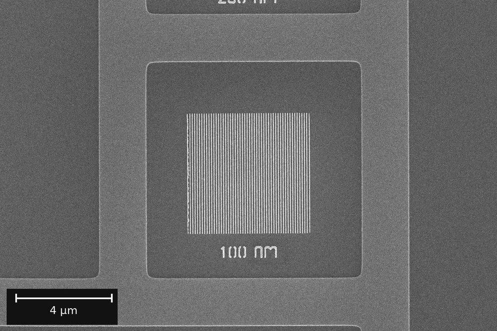
Overview of the calibration standard's 100 nm line set.
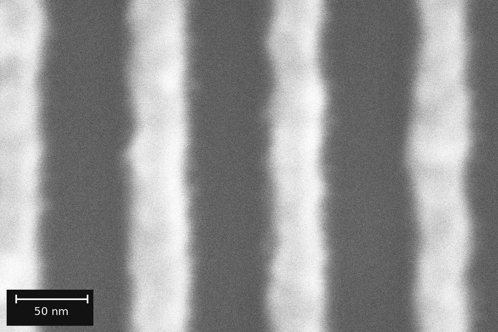
The same calibration standard at higher magnification.

Have a sample and a question?

Email a short description, and a photo if you have one. We reply within one business day with a quote, or with questions if we need more detail.