Materials characterization and failure analysis, scoped by PhD scientists.
Electron microscopy is our core strength, alongside surface, structural, chemical, and thermal analysis: SEM, EDS, FIB-SEM cross-sections, TEM, XPS, XRD, FTIR, and more, for R&D, quality, and failure investigations. Tell us about the sample and what you need to know. We reply within one business day with a fixed quote, or with questions if we need more detail.
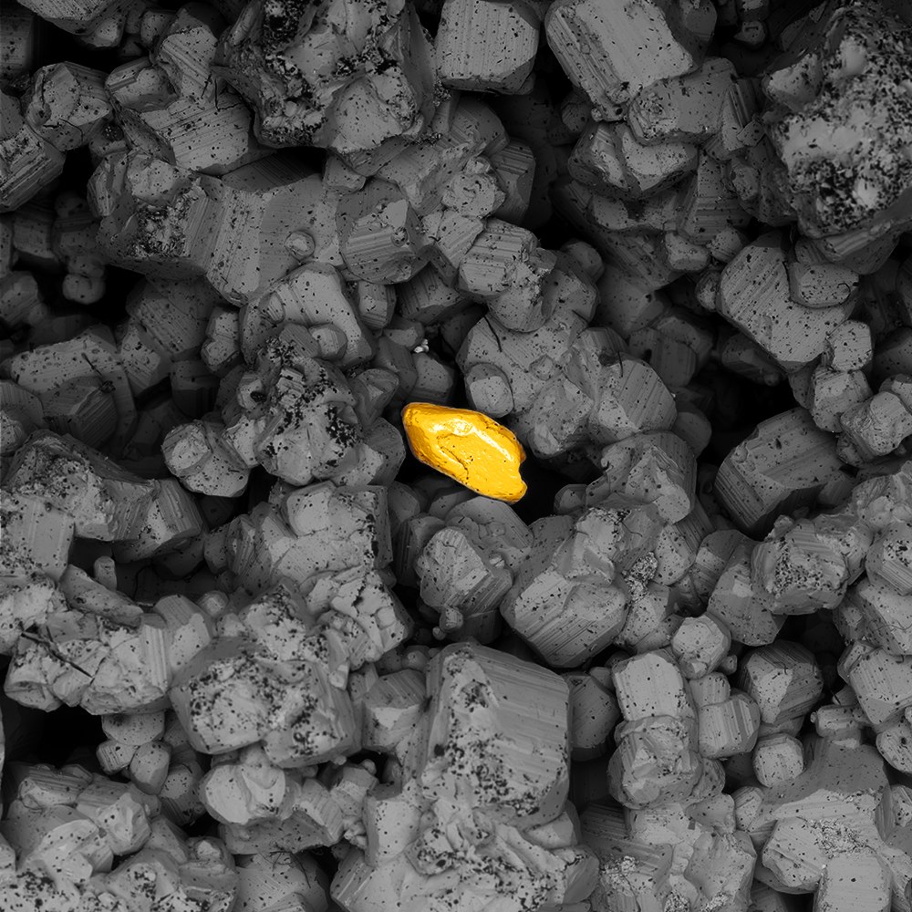
The techniques most materials questions start with.
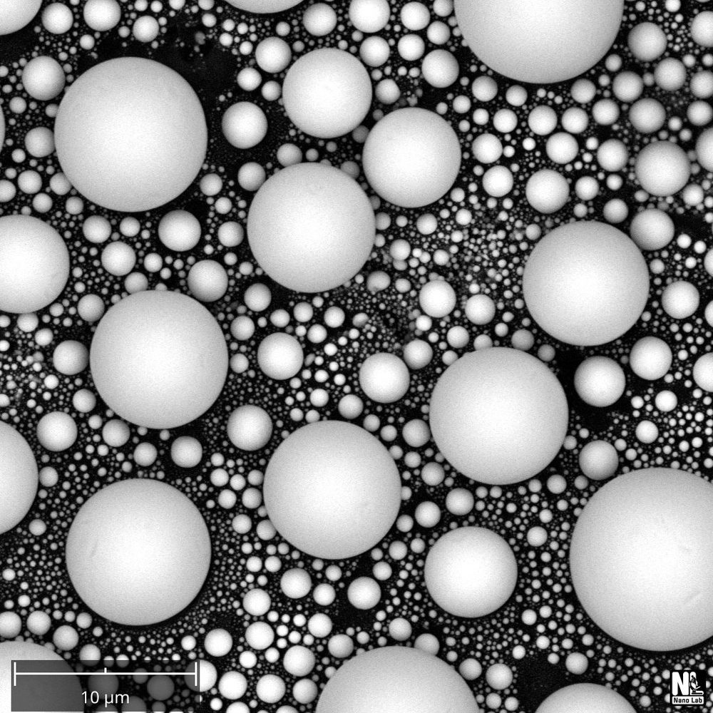
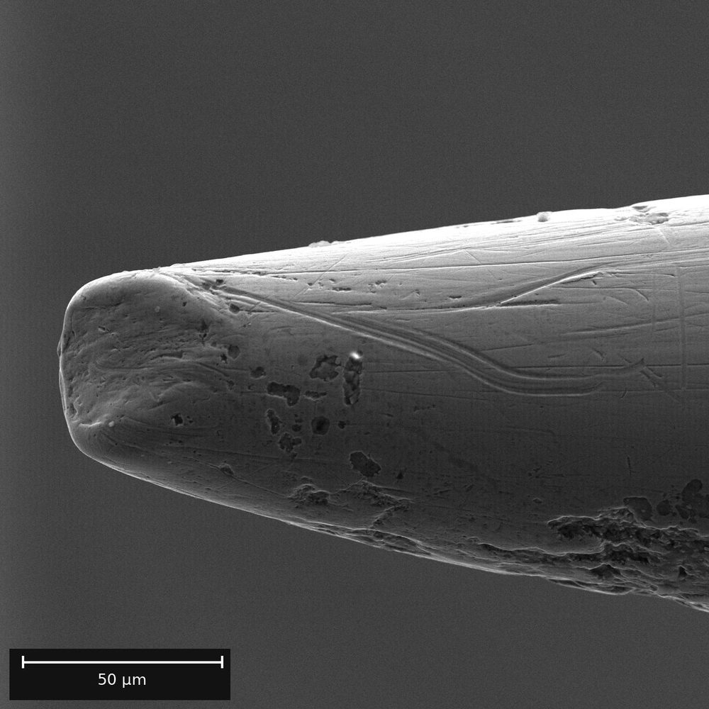
SEM imaging
Surfaces, fractures, particles, coatings, and defects, imaged from millimeters down to nanometers.
EDS elemental analysis
Which elements are present and where: spot analyses, line scans, and maps.
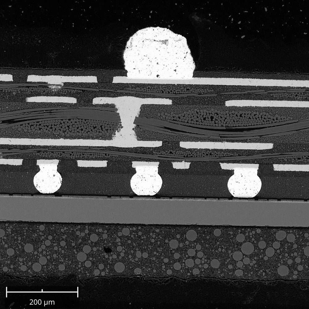
FIB-SEM cross-sections
A site-specific cut through a coating, layer stack, particle, or defect, imaged in place. Cryo-FIB for beam-sensitive materials.
XPS and Auger
Surface chemistry of the top few nanometers: composition, chemical state, and contamination.
X-ray diffraction
Crystalline phase identification and estimated phase fractions.
Surface metrology
Film thickness, step height, and roughness by optical and stylus profilometry and ellipsometry.
Plus TEM, FTIR, Raman, thermal analysis, XRF, particle sizing, and more. All services →
Four steps, in writing.
Tell us the question
Email or use the quote form. Describe the sample and what you need to know. You don't need to know which technique you want; working that out is part of the job.
Get a fixed quote
The scope, a fixed price, and a timeline. We reply within one business day, with the quote or with questions if we need more detail.
Ship the samples
The shipping address comes with the quote. If a sample could be hazardous or biological, tell us before shipping so we can confirm whether and how we can take it.
Receive data and a report
Images, spectra, and data files, with a PDF report of what was observed. Interpretation of the results is available as an add-on.
A small team, led by a PhD scientist.
Your email goes to a PhD scientist who scopes the work with you, reviews the data, and can talk through the results. Founder Caleb Christianson, PhD, brings 17 years of electron microscopy and 6.5 years in medical device engineering, most recently leading failure mode analysis. Being small means fewer handoffs, so you get answers quickly and efficiently.
Most of our work, especially electron microscopy, runs at UC San Diego's Nano3 facility. We usually run the instruments ourselves, and work with trusted specialists for some techniques. We don't own the instruments, which keeps our overhead and prices low and our options flexible, and there is no minimum job size. More about us →
Have a sample and a question?
Email a short description, and a photo if you have one. We reply within one business day with a quote, or with questions if we need more detail.
Or email info@nanolab.llc