
An Introduction to Advanced Material Identification Techniques
EDS, FTIR, Raman, and XRD compared: what each one measures, where each falls short, and which to run first on an unknown.
When you develop a product, you usually know exactly what it's made of. Sometimes, though, you find something you can't identify. An unexpected reaction may be building up a deposit on the surface of a device, or corrosion of a metal part may be contaminating an inner surface. For critical components, or for regulatory reasons, you may need to identify anything unexpected precisely. That can turn into an expensive wild goose chase through one analytical method after another. Should you use FTIR? EDS? XRD? And how do you avoid paying for a full day of work when the right measurement takes thirty minutes? This note lays out a general approach to identifying an unknown material, with the strengths and limits of the most common techniques.
Different spectra, different energies
Most of these techniques are spectroscopic, but they probe very different energies. EDS detects X-rays given off when inner-shell electrons in an atom are knocked out and the vacancies refill. Those transitions involve thousands of electron volts. FTIR and Raman probe molecular vibrations, which involve only a tenth of an electron volt or so, in the infrared. XRD is different again: it relies on X-rays scattering off the regular spacing of atoms in a crystal rather than on an energy transition. Knowing what physical effect each technique measures is the fastest way to pick the right one.
EDS: which elements, and where
Energy-dispersive X-ray spectroscopy, called EDS or EDX, identifies elements. The SEM's electron beam strikes the sample and, among many other interactions, knocks inner-shell electrons out of atoms. When an outer electron drops into the vacancy, the atom emits an X-ray whose energy is characteristic of that element. The detector sorts the X-rays by energy, so the spectrum shows which elements are present and roughly how much of each.
Because the beam can be placed precisely, EDS can analyze a single spot, a line scan, or a full map overlaid on the SEM image. We have used it to map metallization in solder joints and electronic packages, check for contamination on medical device components, and analyze microelectronic cross-sections. More on our EDS service →
The limits of EDS
- Spatial resolution. Electrons spread through the sample before they stop. At typical beam energies, the X-rays come from a volume about a micron across and deep, so the signal can include material below or beside the feature you are aiming at. Lowering the beam energy shrinks that volume.
- Sample requirements. The sample must go into vacuum, so it needs to be dry, free of volatile residues, and small enough to fit. Large parts may need to be cut, which risks contaminating the area of interest. Insulating samples may need a thin conductive coating or a low-vacuum mode.
- Elements only. EDS reports elements, not compounds or molecules. It can't identify a polymer or a petroleum product, because "carbon and oxygen" says very little about which polymer it is.
- Light elements. Hydrogen and helium can't be detected at all, and light elements such as lithium, boron, carbon, nitrogen, and oxygen are detected with lower sensitivity and accuracy.
Beyond elements: FTIR
Many polymers have nearly the same elemental makeup, mostly carbon, hydrogen, and oxygen, so knowing the elements tells you little about their identity. To learn the molecular structure, you need to probe how the atoms are bonded. Molecular vibrations absorb infrared light at frequencies set by the bonds involved. Fourier transform infrared spectroscopy, or FTIR, measures which frequencies a sample absorbs. Large reference libraries of FTIR spectra exist, so an unknown spectrum can often be matched to a known material.[1] FTIR at Nano Lab →
Raman spectroscopy
Raman spectroscopy also measures molecular vibrations, but in a different way. A monochromatic laser illuminates the sample. Nearly all of the scattered light comes back at the laser's wavelength, but a tiny fraction exchanges energy with molecular vibrations and comes back shifted in wavelength. The pattern of shifts is the Raman spectrum, and many materials have characteristic ones.[2]
Raman complements FTIR. Water scatters weakly, so wet samples are easier to measure, and you can measure through glass. Through a microscope it can analyze spots about a micron across, and it is very sensitive to crystal structure. It readily distinguishes graphite, diamond, and amorphous carbon, for example. Its main weakness is fluorescence, which can swamp the much weaker Raman signal in some samples.
X-ray diffraction
The techniques above rely on energy transitions in atoms or molecules. X-ray diffraction relies instead on interference. X-rays scattered from successive planes of atoms in a crystal travel slightly different distances. When that extra distance, 2d sin θ, is a whole number of wavelengths, the scattered waves add up and produce a diffraction peak. This is the Bragg condition, 2d sin θ = nλ, where d is the spacing between planes and θ is the angle of the incoming X-rays.[3]
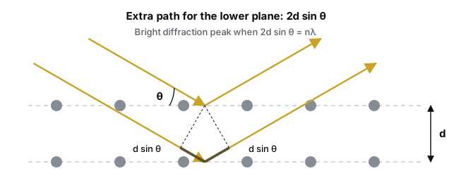
Instead of elements or molecular bonds, XRD measures the crystal structure itself: the set of angles where peaks appear identifies the crystalline phases present and gives information about their orientation. Titanium dioxide is a good example. Its common phases, anatase and rutile, have the same chemical formula, so EDS can't tell them apart, but their crystal structures differ, and so do their optical, electrical, and mechanical properties. XRD identifies each phase and can estimate how much of each is present.[4] Raman can also distinguish the two, but XRD is the standard tool for identifying and quantifying phases. XRD sees only crystalline material; amorphous material gives a broad hump rather than sharp peaks. More on our XRD service →
Choosing the right method
The table below summarizes where each technique fits. For a residue or film on a surface, add XPS, which reads the composition and chemical state of only the top few nanometers. More on XPS →
| Technique | What it tells you | What it can't tell you | Good first choice when |
|---|---|---|---|
| EDS (in the SEM) | Which elements are present, and where, down to about a micron | Molecular identity, chemical bonding, or hydrogen and helium; light elements are less accurate | The unknown is likely inorganic: metals, corrosion, minerals, particles |
| FTIR | Molecular bonds and functional groups, matched against spectral libraries | Elemental makeup of inorganics; very small or very thin deposits can be hard to measure | The unknown is likely organic: polymers, oils, adhesives, residues |
| Raman | Molecular vibrations and crystal structure, often at micron spots | Strongly fluorescent samples can swamp the signal | You need to tell forms of carbon or crystal polymorphs apart, or measure through glass or in water |
| XRD | Crystalline phases and estimated phase fractions | Amorphous material, which gives only broad humps; phases below a few percent are hard to see | You know the elements and need the compound or phase |
| XPS | Composition and chemical state of the top few nanometers | Anything deeper than the surface, unless combined with depth profiling | The problem is a thin film or contamination layer on a surface |
Many related techniques exist, such as X-ray fluorescence and electron energy loss spectroscopy, and each has its own strengths and limits. But knowing what the common techniques measure, and what they can't, lets you approach an unknown material with confidence and avoid paying for measurements that can't answer your question.
Have an unknown residue or deposit?
Send a photo and a short description of where it appeared. We'll suggest the measurement most likely to answer the question first, and quote a fixed price before anything ships. There is no minimum job size.
References
- P. R. Griffiths and J. A. de Haseth, Fourier Transform Infrared Spectrometry, 2nd ed. (Wiley, 2007).
- E. Smith and G. Dent, Modern Raman Spectroscopy: A Practical Approach (Wiley, 2005).
- S. H. Simon, The Oxford Solid State Basics (Oxford University Press, 2013), p. 143.
- B. D. Cullity and S. R. Stock, Elements of X-Ray Diffraction, 3rd ed. (Prentice Hall, 2001).