
Performing FIB on Extremely Rough Surfaces
Why rough surfaces make FIB cross-sections hard, and two ways to get a clean sidewall anyway.

Focused ion beam (FIB) milling is one of the most reliable ways to see below the surface of a device. Paired with SEM imaging and EDS, it can measure the dimensions and composition of an entire layer stack at a chosen spot. Most of the time we cut into a flat surface, such as a metal pad or a passivation layer. Sometimes the surface is far from flat, and a very rough surface makes ion milling much harder.
Protruding features can block the view of the cut, because the electron beam images the face at a tilt. Deep ridges and valleys change the local angle of the ion beam, so different parts of the cut mill at different rates. Some products are rough on purpose. Dental restorations, for example, are often sandblasted or acid etched so that cements bond to them.
![Acid-etched surface of a CAD/CAM resin-matrix ceramic, SEM.<sup><a href="#ref-1">[1]</a></sup>](/assets/img/notes/resin-ceramic-etched-surface.jpg)
The challenge
Suppose a sintered metal part has a thin coating, and you need the coating's profile in cross-section. If the RMS roughness is in the micron range, you have to be strategic about where you cut and what kind of cut you make, and you may need a thick protective platinum layer first. Low-current, multi-pass cuts give the most control, but they take time, and time matters when cross-sections are needed several times a day.
Gallium FIB systems use a liquid metal ion source, with ions typically accelerated to 30 kV. Gallium ions are heavy enough to mill nearly any solid, including hard composites and metals. But a beam scanned over a region with mixed materials and varying height mills unevenly and leaves curtaining on the face. Extreme roughness magnifies both effects, sometimes to the point that even a cleaning cut can't produce a usable sidewall. This note covers why that happens and two ways to deal with it: a careful, surgical cut, and a fast alternative that buries the roughness under a thick metal cap.
Why the milling angle matters
The milling rate depends strongly on the angle between the ion beam and the surface. At normal incidence, with the beam perpendicular to the surface, much of each ion's momentum is driven into the material. The energy is spread through the lattice below rather than ejecting atoms from the surface, so material comes off relatively slowly.
When the beam strikes at a glancing angle, more of the collision cascade stays near the surface, and more atoms gain enough energy to escape. More atoms are sputtered per ion, so the surface mills faster.[2]
![At normal incidence (a), momentum is carried into the lattice. At oblique incidence (b), more surface atoms are ejected per ion. Schematic after reference [2].](/assets/img/notes/ion-incidence.svg)
The exact angle of peak sputter yield varies with the material and the beam energy, but for many common materials, silicon included, it falls at roughly 70 to 80 degrees from the surface normal. Past the peak, the yield falls off sharply, because ions start to glance off the surface instead of entering it. Measured curves for tungsten carbide and cobalt follow the same shape.[3]
![Sputter yield rises with angle of incidence, peaks at roughly 70 to 80°, and drops steeply toward grazing incidence. Schematic; the exact curve depends on the material and the beam energy. See reference [3] for measured data.](/assets/img/notes/sputter-yield-angle.svg)
This is why a protruding feature with a flat top is hard to mill evenly. The flat top and the flat floor around it both see the beam at normal incidence and mill slowly, while the sloped sides mill quickly. The feature shrinks sideways faster than it gets shorter, and a plateau survives even after a lot of milling.[4] On a rough surface, milling a large area can leave behind pillars and protrusions with flat tops for the same reason.
![A flat-topped feature under the ion beam. Flat surfaces mill at the slow, normal-incidence rate and sloped faces mill faster, so a plateau persists. Schematic after reference [4].](/assets/img/notes/milling-plateau.svg)
Curtaining and redeposition
Beyond the angle effect, curtaining and redeposition can leave a rough, low-quality sidewall. Curtaining shows up as vertical streaks running down the face, below bumps on the surface and below changes in density within the sample. Redeposition is sputtered material settling back onto the face. Both are common on large cuts through porous or rough material.[5]
![Curtaining: features at the top of the cut shadow the beam and leave vertical streaks down the polished face. Schematic; see reference [5] for SEM images on a porous surface.](/assets/img/notes/curtaining.svg)
Because curtaining is tied to the beam's direction, some newer FIB systems can rock the stage, changing the milling angle slightly back and forth during the cut to smear the streaks out. Where rocking isn't available, the usual remedies are a protective metal cap over the region of interest, discussed below, and finishing with a lower-current cleaning cut.
Option 1: a small, surgical cut
One approach is to use a lower beam current, more passes, and a smaller cut tuned to the local topography. For example, you can first remove the front of a tall ridge so it doesn't block the tilted SEM view, then cut a small section off the targeted ridge to get a cleaner sidewall.
The trade-offs are real. A typical higher-current cut might take a couple of minutes, while a careful, low-current cut can take tens of minutes or more. When cost and speed matter, that may not be practical. On ridges with strong curvature, the local angle of incidence changes across the surface, so the mill rate changes too, and the geometry has to be accounted for to get consistent results. Doing this well on very rough samples takes real experience, which adds further time and cost.
Option 2: bury the roughness under a thick cap
Several questions decide whether a protective layer is needed. Will the film be damaged by the ion or electron beam? Is there charging, drift, or another beam artifact? If so, depositing metal, usually platinum, over the area helps, and it also evens out some of the effect of surface roughness on the cut. A thin coating often isn't enough on a very rough surface, though, and curtaining and uneven milling can persist. Deposition also adds time, especially electron-beam deposition, which is slow.
The alternative is a much thicker platinum cap, microns thick, laid down mostly with the ion beam at higher current. A thin electron-beam layer goes on first to protect the surface from the ion beam. As a rough guide, a surface with about 2 µm of roughness may need a 3 to 5 µm cap to leave a smooth top over the whole cut. The cap adds time, but it gives a much cleaner sidewall with far less curtaining, and you can cut a much wider cross-section than a surgical cut would allow. A typical flow, depositing platinum from a gas injection needle:
- Deposit a thin electron-beam platinum layer, about 300 nm or less, over the region of interest.
- Tilt the stage and deposit about 1 µm of platinum with the ion beam at moderate current.
- Build up the rest of the cap with the ion beam at higher current, to a total of several microns if the roughness needs it.
- Mill a wide trench at high current, working toward the face you will image, placed under the middle of the cap.
- Finish with a lower-current cleaning cut on the exposed face.
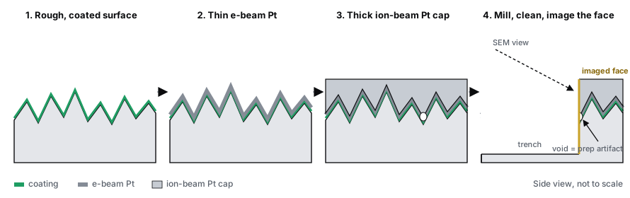
This flow protects surface coatings and is faster than low-current, multi-pass approaches. It also exposes a wide stretch of the sidewall, so you can see the larger-scale topography of a coating or structure, not just one spot.
It has limits. A large, high-current cut can damage the surface nearby and cause significant redeposition, so it is a poor fit for sensitive samples or areas that need to be imaged again later. The cap may also fail to fill the bottoms of deep valleys, leaving voids between the platinum and the sample. Those voids are preparation artifacts, not part of the device profile, and they should be labeled as such in any report. Imaging selected regions of the face can keep them out of the final images.
Choosing an approach
FIB remains one of the most powerful and versatile techniques for nanoscale cross-sections, even on difficult surfaces. On very rough samples, a metal cap is often what protects the films, prevents charging and drift, and keeps the cut even. The right choice depends on how much time the analysis can take, how much of the sidewall you need to see, and how sensitive the surface is. Understanding those trade-offs lets you match the cross-section plan to what the question actually requires.
FIB-SEM cross-sections at Nano Lab
We cut site-specific FIB cross-sections through coatings, layer stacks, particles, and defects, with cryo-FIB available for beam-sensitive materials. Send a photo or a description of your surface, and we'll suggest a cross-section plan with the quote.
References
- H. A. Muhammed, E. M. Mahmoud, A. E. Fahmy, D. M. Nassar, "The effect of sandblasting versus acid etching on the surface roughness and biaxial flexural strength of CAD/CAM resin-matrix ceramics," BMC Oral Health 23, 169 (2023). doi:10.1186/s12903-023-02883-6
- Materials and Manufacturing Processes (2012). doi:10.1080/10426914.2011.654166
- A. Goswami, R. Umashankar, A. K. Gupta, S. Aravindan, P. V. Rao, "Development of a microstructured surface using the FIB," Journal of Micromanufacturing 1(1), 53–61 (2018). doi:10.1177/2516598418765357
- Journal of Microscopy (2007). doi:10.1111/j.1365-2818.2007.01737.x
- PubMed 32438937. pubmed.ncbi.nlm.nih.gov/32438937